
Quite a while back I designed a small PCB for hooking up sensors to an ESP8266 module to gather data and have a nice Grafana dashboard with temperature readings. While building this setup I grabbed one of my spare ESP8266 dev boards and soldered that to the P1 port on my smart energy meter to log the power usage of the whole house.
For those unfamiliar with P1 and DSMR since it's quite regional: DSMR is the Dutch Smart Meter Requirements specification. It's a document that describes the connectivity of various ports on energy meters and it's used in the Netherlands and a few countries around it. One of the specifications within DSMR is P1 which is the document for the RJ12 connector for plugging third party monitoring tools.
Electrical design
So the first part in the project is figuring out how to make the hardware itself work. I've decided to slightly modernize my design so this is the first module I build that uses an ESP32 chip instead of the older ESP8266 I have in use everywhere.
I specifically designed the board around the ESP32-S3-WROOM-1 module. This makes things significantly simpler than my older designs since there's no programming circuitry required.
The design contraints I've used for this board are:
- Make the design handsolderable instead of using JLCPCB assembly service for the boards. I enjoy designing boards and I probably should get some more actual soldering experience with SMD parts.
- Connect to the smart energy meter using off the shelf RJ12 cables instead of soldering wires on the board. Also include a passive P1 splitter on the board since it's becoming more and more popular to have charging points for electric cars which can also be hooked up to the P1 port.
- USB-C for programming and power. I have a back-up programming header footprint on the board but it shouldn't be necessary . Just like putting USB-B Micro ports on devices shouldn't be allowed anymore in 2024.
The schematic is basically the absolute minimum required to get the ESP32 module up and running. Since the ESP32-S3 has native USB support it means that I can drop a whole bunch of parts from the schematic that is normally required for programming.
Another neat feature is that this chip has a fully connected I/O mux inside which means I can basically pick any random GPIO pin and later configure in software which hardware block in the chip it hooks up to. This feature is also available in other chips like the RP2040 but there it's way more limited. There is only a few valid choices for pins for UART1 for example and there's no way to swap RX and TX on a board without using a soldering iron.
In the DSMR design I'll only be using a single GPIO pin configured to be the RX of one of the hardware UARTS so it can receive the data.

The board has a jumper on it to pick how the data requests are handled. In one position the line is connected straight to 5V so the energy meter will just continuously send the data over the P1 port, which should be correct in most situations. The other mode connects the data request line to the pass-through port so the device connected after the DSMR module can select when the data should be sent, in this case the module will just be passively sniffing the traffic whenever it's sent.
There is also a solder jumper on the board to select whether it's powered from the USB connection or from the P1 port itself. According to the P1 specifications the power supplied by most energy meters won't be enough to reliably run the ESP32 module so there is always to option to power it from the USB-C port. In most cases there will be random device like a router nearby that has a powered USB connection to run the module.
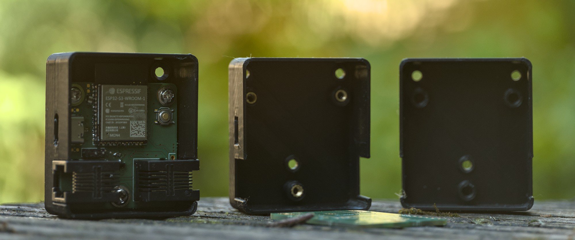
I managed to fit everything on a small 40x40mm PCB by having the the two RJ12 connectors hang off the board. This also makes those neatly line up with the edges of the case for this board. The ESP32 module also hangs off the edge of the board, pictured at the top here. This is because the antenna part of the ESP module has a keepout area where there shouldn't be any copper on the board anyway to not disturb the WiFi signal.
To make it fit I've also moved the power regulator and a few passives to the bottom side of the board. Normally it would be pretty expensive to do this but since I'm hand soldering these boards using both sides of the board is free.
Another upside with handsoldering the boards is that I'm not limited to the JLCPCB parts for once and I can just whatever random parts I can source. I've decided to get these boards made by Aisler this time so the boards are made in Germany instead of China and the boards just look great. I normally use the KiCad Aisler Push plugin in my workflow anyway just to run some sanity checks on the board design in addition to the checks ran in KiCad.

In this screenshot it's just warning me about the holes for the plastic pins in the footprint of the USB-C connector. It doesn't matter whether those are copper plated or not so I just ignore this warning. After receiving the boards I've also checked this and the holes did not get copper plated at all.
I also noticed there was a discount for using components from Würth Elektronik on the board so naturally I took that as a challenge to see how for I can push that. It turns out that in this design the answer is pretty far: The easy thing is to use WE part numbers for the passives on the board.
The second thing I replaced is the connectors on the board. I was already pretty happy I did not have to make custom footprints for once because that's just a time consuming job. After comparing a lot of footprints it turns out that WE makes an RJ12 connectors with the exact footprint I had already made. The USB-C connector is a bit more difficult since I'm used to picking the one available at JLCPCB that also happens to have a footprint already in KiCad. It turns out that the Würth Elektronik USB-C connector fits on the USB_C_Receptacle_GCT_USB4105-xx-A_16P_TopMnt_Horizontal footprint in KiCad. I guess there's simply not too many different ways to make spec compliant USB-C connectors.
The soldering
So the board is relatively straightforward to solder, it doesn't have that many parts and I decided to not pick the tiniest SMT parts I could find. If you're not familiar with SMT parts, they get delivered on reels and if you order small quantities you get a smaller cut-off portion of a reel. Here's some capacitors for example:

These are the 22uF 0805 capacitors I've ordered for the ESP32 power rail. The rest of the passives are the slightly smaller 0603 packages. On the right of the board you can see the pads for the 0805 capacitor and the 0603 capacitor side by side. In this case the Würth capacitors came in a neat transparent piece of tube. If you order a full reel of cheap resistors they usually come on paper tape which looks like this:

This is probably one of few times I've ever ordered 5000 of something. Even the bigger parts like the ESP32 modules come on a reel:

This soldering itself was quite time consuming but not that hard. The secret is to just use a lot of flux and not use plastic tweezers that melt while soldering.

Maybe after some experience I can even get them on straight. Supposedly it's a lot easier and neater to use solder paste and stencils to do this so I also ordered the stencils for this PCB. I don't have the soldering paste and extra equipment for it though so that experiment will have to wait a bit longer.
The case
To have this look somewhat neat when it's finished I also need a case for the board. The need for cases has annoyed me several times already when designing PCBs. The options are either grabbing an off the shelf project box which is usually expensive and never fits exactly with the design or just 3D printing a case which involves me angrily staring at CAD software to figure out how to make things fit and match up to my PCB.
I've already written a blog post about my solution here which is TurboCase. It's a tool that automatically generates a case based on the PCB file from KiCad. I wrote the software specifically because I needed it for this PCB so naturally the case generated by it works perfectly for this project :)

Since writing the blog post about the details on how TurboCase works I've added support for TurboCase-specific footprints. I now have a global KiCad library that holds footprints that are designed to go on the User.6 layer to add prefab features to the final OpenSCAD file like screw holes in the case and the hole for by USB-C connectors.

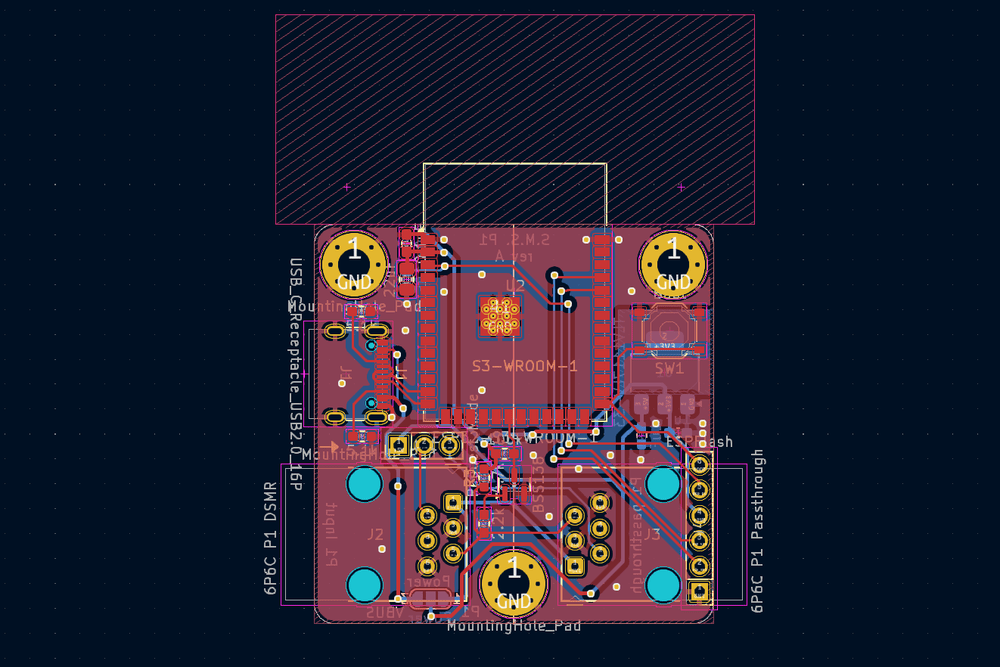
Here you can see the drawing on the User.6 layer of the DSMR module. It contains several features:
- The outline of the case drawn using the graphic elements in KiCad. This functions the same way as the board outline normally works on the
Edge.Cutslayer except it describes the outline of the inside of the case. - Three mounting holes that fit countersunk M3 sized screws to mount the case on the wall.
- A M3-sized keyhole screw-mounting thingy so the board can be mounted in a less permanent way.
- The cube with the line in it marks a spot where turbocase makes an USB-C shaped hole matched up perfectly to the USB-C connector on the board.
- The RJ12 connectors already cross the border of the case in KiCad so there will be holes generated for them automatically in the case based on the connector outline on the fabrication layer.
- The 3 MountingHole footprints on the PCB will be used to generate mounting posts for the PCB inside the case, the main reason why I started making this tool to make sure those things align perfectly every time.
I did a few iterations on the footprint library and did a series of test prints of the case to make sure everything is correct and I can happily report that everything just matches up perfectly.
The few days I spend building and testing this tool now narrows down the whole process from kicad to physical product down to:
- Draw outline in KiCad
- Run TurboCase on the
.kicad_pcbfile to get my OpenSCAD file. - Export the OpenSCAD file to .STL and 3D print it.
I hope this utility is useful for more people and I would love to see how it performs with other board designs!

The software side
The more annoying part of the whole process was dealing with the software. For the ESP8266 I've always used the Arduino IDE. This is mainly because I did not want to deal with the xtensa toolchain required to build software for these chips. I don't do complicated things with these modules and with the Arduino IDE they simply always just worked.
Switching over to the ESP32 did mean that stuff stopped working automatically for me sadly, the base software worked great but I had some troubly getting the MQTT library to work. The dependency resolution in the Arduino IDE is very simple and it does not account for having different dependencies with the same include name so I tried PlatformIO for this project.
The whole setup process for PlatformIO was pretty smooth until I got to platform selection. There's a few different variations of the ESP32-S3 module available and even a few more specific variations of the WROOM-1 module I put on my board. I dit however commit the sin of picking the 4MB flash version of the board. This is the only one that doesn't have a specific config in PlatformIO and the merge request for it was denied based on that it would be easy to override the platform config with a json file. I did not find how to do that easily so I picked one of the random dev boards that used the wroom-1 module with 4MB flash instead to use whatever changes they have made to the JSON file for the board to make this work.
Now for actually implementing the P1 protocol: This is deceptively hard. The way the protocol works is that you pull the data request line high on the connector and then the energy meter will start spewing out datagrams over the serial port on either a 1 second or 10 second interval depending on the protocol version. These datagrams look something like this:
/XMX5LGBBFG10

1-3:0.2.8(42)
0-0:1.0.0(170108161107W)
0-0:96.1.1(4530303331303033303031363939353135)
1-0:1.8.1(002074.842*kWh)
1-0:1.8.2(000881.383*kWh)
1-0:2.8.1(000010.981*kWh)
1-0:2.8.2(000028.031*kWh)
0-0:96.14.0(0001)
1-0:1.7.0(00.494*kW)
1-0:2.7.0(00.000*kW)
0-0:96.7.21(00004)
0-0:96.7.9(00003)
1-0:32.32.0(00000)
1-0:32.36.0(00000)
0-0:96.13.1()
0-0:96.13.0()
1-0:31.7.0(003*A)
1-0:21.7.0(00.494*kW)
1-0:22.7.0(00.000*kW)
0-1:24.1.0(003)
0-1:96.1.0(4730303139333430323231313938343135)
0-1:24.2.1(170108160000W)(01234.000*m3)
!D3B0
This looks to be a relatively simple line based protocol. The fields are identified by a numeric code called the "OBIS" code. This stands for OBject Identification System. Then there's values added in parenthesis after it. The difficulty in parsing this is that there can be multiple values in parentheses added after each OBIS field. This would not be terrifically hard to parse if the DSMR spec had nailed down the encoding a bit more but it merly specifies that the field ends in a newline.
In my case some of the values themselves also contain newlines so this breaks the assumption you can parse this based simply based on lines and that combined by the variable (but unspecified) amount of values means that the parser code for this becomes quite nasty.
Luckily I got to use one of the features I gained by switching to PlatformIO: Unit testing. The whole DSMR parser is moved to it's own class in the codebase and only gets a Stream reference to parse the DSMR datagrams from. This means I don't have to sit with my laptop in the hallway debugging the parser and I can check if the parser works with dumps from various smart energy meters.
This all glued together means that the DSMR module will get the data from the P1 port and then sent it out over WiFi to my MQTT server with a separate topic for every field. And the result:

The source for the hardware and firmware is available at https://git.sr.ht/~martijnbraam/dsmr-module and the board itself is also available on https://aisler.net/p/IWCEGPWL