
I don't generally get along great with CAD software with the exception of KiCad. I guess the UX for designing things is just a lot simpler when you only have 2 dimensions to worry about. After enjoying making a PCB in KiCad the annoying for me is always getting a case designed to fit the board.
If I'm lucky I don't need many external holes to fit buttons or connectors and if I'm really lucky the mounting holes for the board are even in sensible locations. I wondered if there was a quick way to get the positions of the mounting holes into some 3D CAD software to make the mounting posts in the right position without doing math or measuring.
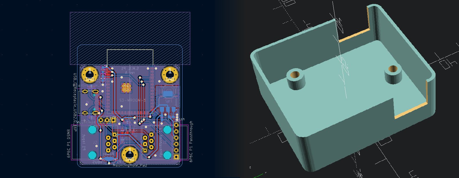
But what's even better than importing mounting hole locations? Not having to build the case at all!
Turbocase
So the solution is just several hundred lines of Python code. I've evaluated a few ways of getting data out of KiCad to mess with it and initially the kicad-cli tool looked really promising since it allows exporting the PCB design to several vector formats without launching KiCad. After exporting a few formats and seeing how easy it would be to get the data into Python I remembered that the PCB design files are just s-expressions, so the easiest way is just reading the .kicad_pcb file directly.
So with this there's several pieces of data the tool extracts for the case design:
- The footprints with
MountingHolein the name to place posts for threaded metal inserts in my 3d prints - A case outline from a user layer. This has the same semantics as the Edge.Cuts layer except that it defines the shape of the inner edge of the case.
- Information about connectors to make holes in the case and to have placeholders in the final OpenSCAD file for easier modifications.
The locations of the mounting holes is pretty easy to get up and running. By iterating over the PCB file the tool saves all the footprints that are mounting holes and for each of those footprints it locates the pad with the largest hole in it and saves that to make a mounting post in the case.

In my test PCB I already had some nice edge-cases to deal with since the specific footprint I used has vias in it which also counts as pads. The outer side of the pad is used as the diameter of the mounting post that will be generated and inside that a hole will be created that fits the bag of threaded metal inserts I happen to have here.
Case outlines
To make the actual case I initially planned to just grab the PCB outline and slightly enlarge it as a template. This turns out to have a few obvious flaws, for example the ESP32 module that I have hanging over the edge of the PCB. Grabbing the bounding box of the entire design would also be a quick fix but that would mean the case would be way too large again due to the keepout area of the ESP32 footprint. The solution is manually defining the shape of the case since this gives the most flexibility.
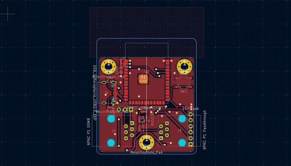
I picked the User.6 layer as the case outline layer since it has a neat blue color in this KiCad theme. The semantics for the case outline is the same as what you'd normally do on the Edge.Cuts layer except that this defines the inner wall of the case. The turbocase utility will then add a wall thickness around it to make the 3D model of the case.
Connector holes
What use is a case without any holes for connections? This turned out to be a more difficult issue. For the connectors I would actually need some height information and KiCAD is still very much 2D. It is possible to link a 3D model to the footprint which is great to see how the final board will look like:
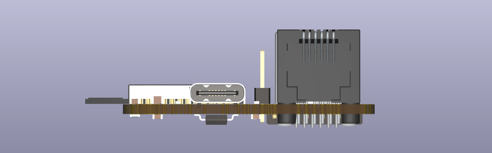
Sadly using this 3D model data would be quite difficult for turbocase since it would require an importer for all the various supported 3D model formats and then a way to grab the outline of a slice of the model.
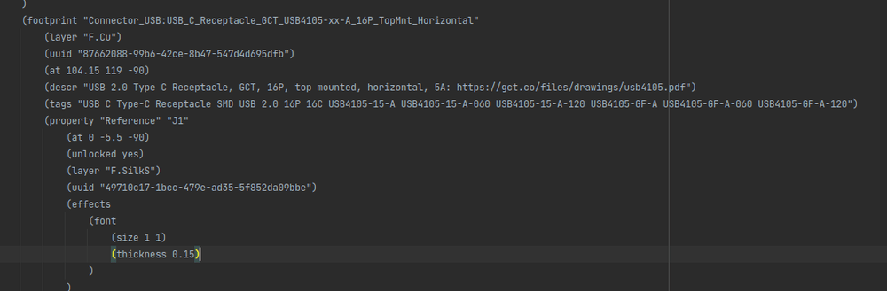
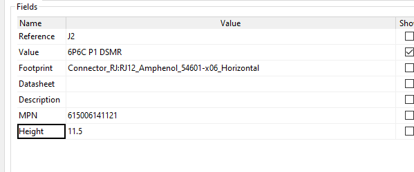
So I picked the uglier but simpler solution. Just give the connector a height in some metadata and treat them as cubes. For the footprint I use the bounding box of the F.Fab layer which should correspond relatively closely to the size of the connector. To store the 3rd dimension I simply added a property to the connectors I wanted to be relevant to the case design:
Exporting the case
I decided to export the cases as OpenSCAD files. This is mostly because these are simple text files I can generate and I already have some experience with OpenSCAD design.
A large part of the generated file is boilerplate code for doing the basic case components. After that it will export the case outline as a polygon and do the regular OpenSCAD things to it to make a 3D object.
standoff_height = 5;
floor_height = 1.2;
pcb_thickness = 1.6;
inner_height = standoff_height + pcb_thickness + 11.5;
pcb_top = floor_height + standoff_height + pcb_thickness;

box(1.2, 1.2, inner_height) {
	polygon(points = [[102,145], [140,145], .... ]);
}
The pcb_thickness is also one of the variables exported from the KiCad PCB file and the box(wall, bottom, height) module creates the actual basic case.
For the connector a series of cubes is generated and those are substracted from the generated box:
// J1 Connector_USB:USB_C_Receptacle_GCT_USB4105-xx-A_16P_TopMnt_Horizontal USB 2.0-only 16P Type-C Receptacle connector
translate([104.15, 119, pcb_top])
  rotate([0, 0, 90])
    #connector(-4.47,-3.675,4.47,3.675,3.5100000000000002);

// J2 Connector_RJ:RJ12_Amphenol_54601-x06_Horizontal
translate([115, 131.9, pcb_top])
  rotate([0, 0, 90])
    #connector(-3.42,-1.23,9.78,16.77,11.7);

// J3 Connector_RJ:RJ12_Amphenol_54601-x06_Horizontal
translate([127.11, 138.26, pcb_top])
  rotate([0, 0, 270])
    #connector(-3.42,-1.23,9.78,16.77,11.7);
This also has some extraced metadata from the PCB to figure out what's what when editing the .scad file. The connector module is a simple helper for generating a cube from a bounding box that accounts for the origin of the connector not being in the center.
Finally the mounting posts are added to the case as simple cylinders:
// H1
translate([105, 108, 1.2])
	mount(3.4000000000000004, 6.4, 5);

// H3
translate([121, 140, 1.2])
	mount(3.4000000000000004, 6.4, 5);

// H2
translate([137, 108, 1.2])
	mount(3.4000000000000004, 6.4, 5);
The extracted information from the mounting hole is the 3.2mm drill diameter and the 6.2mm pad diameter. The inner hole is expanded by 0.2mm in this case to make the holes work with the metal inserts.
Further improvements
There's a lot of neat things that could be added to this. The major one being a lid for the case. This also would need a bunch more configurability to deal with mounting mechanisms for the lid like screw holes or some clips.
The system could also be extended by producing a footprint library specifically for turbocase to signify where to add specific features to the case. This could be things like cooling holes, led holes. Maybe some fancier connector integration.
The output from turbocase also suffers from the same issue a lot of OpenSCAD designs suffer from: it's very hard to add chamfers and fillets to make a less rectangular case. That would require someone with more OpenSCAD knowledge to improve the generated output.
The source code for the turbocase tool is available at https://sr.ht/~martijnbraam/turbocase/ and the utility is available on pypi under the turbocase name.