
I do a lot of software development, I do enough of it to be comfortable with the process. I have worked on enough projects and have made enough pieces of software that it's quite easy to quickly spin up a new project to fix a specific issue I'm having.
Hardware design is a whole other can of worms. I have played with things like the Arduino and later the STM32 chips, ESP8266 and RP2040. These things are quite neat from a programmers perspective. You write your code in c++ and the included toolchain figures out all the hard parts and flashes the board. Hardware design is also quite simple since it's mostly putting together different hardware modules and breakout boards. Only a basic understanding of the hardware busses is required to get stuff up and running.

Projects usually look like the picture above. No resistors, capacitors or other components are needed. Just a breadboard (also optional), jumper wires and the IO modules you need to make your idea work.
Power is dealt with by the microcontroller board, the modules already include the pull-up resistors and power regulators required and the programmer is also included already.
The software side is also simplified and abstracted to the point where it's harder to get your average javascript project working than the embedded projects. You'd never have to open the 440 page atmega 328p manual to write the firmware. You don't even need to know about the register map for GPIO pins since things like digitalWrite(pin, state) exist.
It's easy to get a complete prototype running like this but then what?
Putting things in production
By far the easiest way to put the project in production is just shoving the breadboard in a project box and declaring it done. It works but it's not neat. This works if you only need one and it's for yourself.
When you need 5? 10? 30? of the same thing then breadboarding it will become a lot less practical. In some cases it's easy enough to just stick the modules on a piece of protoboard and solder it together. When that doesn't scale another option is putting the modules on a custom PCB.
This is exactly what I did for a project. This is the first PCB I have ever designed and put into production:


It's a PCB that only has pinheaders and connectors on it. This board would have a nodeMCU module and an off-the-shelf rs485 module on it. The board itself is incredibly simple but it did give me a chance to run through the complete process of going from a schematic to an actual physical product. Since it has no actual components on it it has removed a lot of worry if the board will work at all.
In this case the board was designed because I needed 15 of this design and this makes a lot more reliable and easy to maintain with the possibility to have neat screw terminals on it for the external connections.
Optimizing the design more
The above design was simple enough to not worry about optimizing it, but another project I wanted to take on is replacing my various sensor nodes with a neater custom design.


These boards have been put together around various ESP8266 dev boards, most of them are nodeMCU v3 boards, some are off-the-shelf boards that I receive data from with an rtl-sdr.
My plan is to make the one board to rule them all. A custom designed board that makes it easy to connect my existing sensors and allows a bit of extension. The design is based around an ESP-12F module since all my existing sensor code is already written for the various ESP8266 boards. It's also in stock at LCSC so that makes it a lot easier to get fabricated.
The design goals for this custom board is:
- On-board programmer for development
- Have the ESP module hooked up so it can deep sleep properly
- Have a built in temperature sensor. Most of my external sensor boards are already temperature/humidity sensors so it makes sense to just include it since it's a cheap chip.
- Have a screw terminal for hooking up onewire devices
- Expose a silkscreen marked SPI and I2C bus
- Be able to be powered with an USB Type-C cable or a single lithium cell.
- Have a built-in charger for the lithium cell.
- The board should be able to be assembled by JLCPCB and Aisler
For implementing this I mostly looked at the nodeMCU v3 schematic as reference and also made the basic layout of the PCB similar to that board. Initially I wanted to add the very popular DS18B20 onewire temperature sensor on-board but that got replaced with the SHT30 module that also includes a humidity sensor and connects to the I2C bus instead.
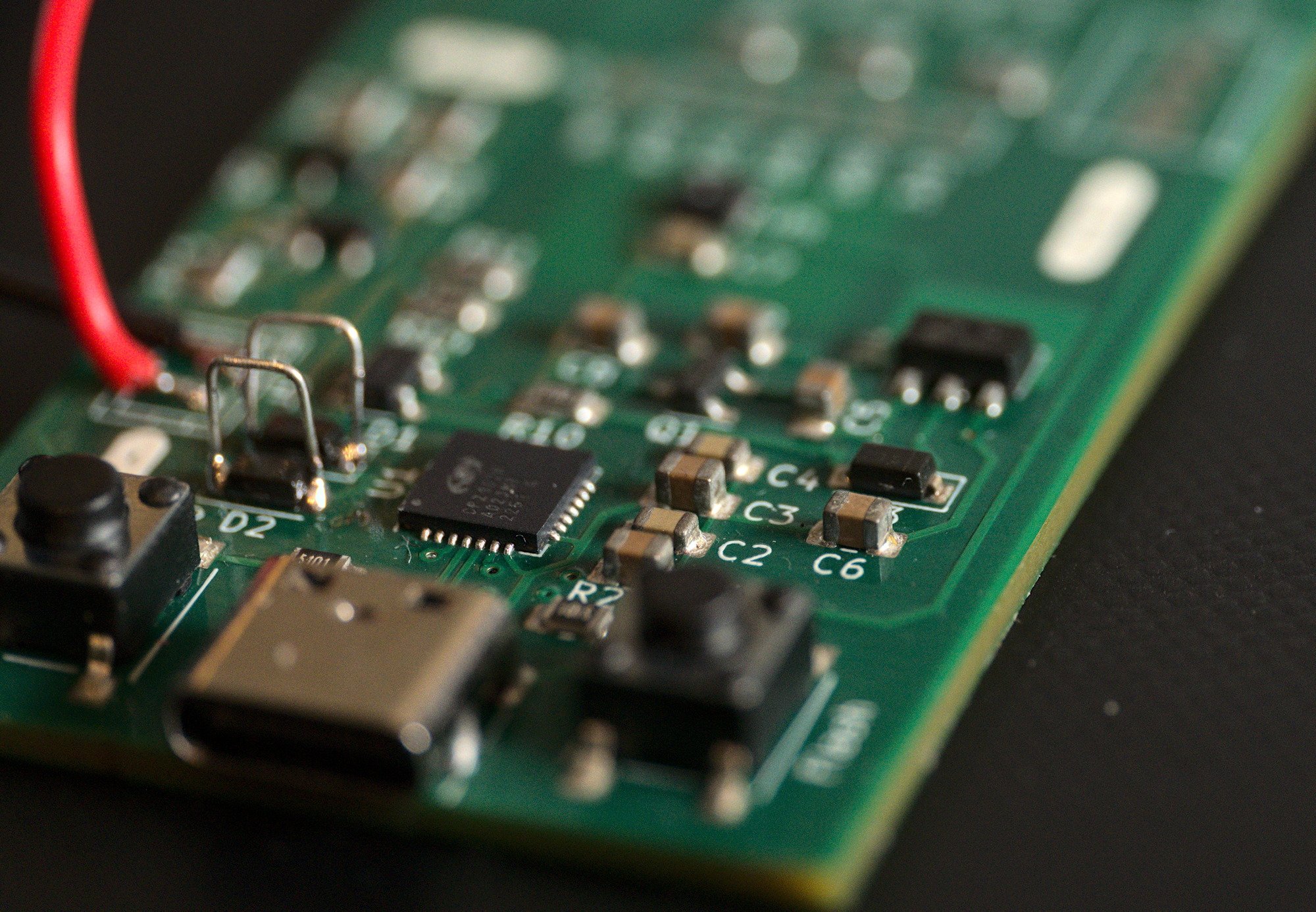
For the programming and USB part I included the CP2102 USB-to-serial converter chip that was also included on the nodeMCU board. It is probably overkill for this application though since I'm not using any of the functionality of that chip beside the RX/TX pins. I dropped the auto-reset circuit since I was worried it would interfere with the deep sleep reset circuit that I found more important.

One simple change from the nodeMCU design is that I swapped the USB Micro-B connector for a Type-C connector which requires a bit more PCB routing to deal with the reversable plug and two extra resistors to make it up to USB spec. The Type-C spec requires a 5.1kΩ resistor to ground on both CC pins (individually, don't cheap out and connect both CC pins to the same resistor like on the Raspberry Pi)
Most of this design work is simply reading the datasheets for the components and following the recommendations there. Some datasheets even have bits of recommended PCB layout in it to make the PCB layout easier.
Since all the complicated ESP8266 circuitry is already handled on the SoM I used and the USB-to-serial converter is laid out, the rest is simple connectors. Except... there's power stuff to deal with.
Most of the difficulty with this design is figuring out the power design. If the battery connection was not included it would've been relatively straightforward. Just have a power regulator that converts the 5V from the USB connector to the 3.3V for the rest of the board. This is exactly what the nodeMCU board does.
In my case the regulator has to deal with power coming from either USB or a single Lithium bringing the input voltage range from 3.4-ish to 5V. There's also a charger chip included to charge the connected cell and a bit of circuitry to switch between the battery and USB power.

The diagram above shows the final power design. It has the MCP1700 3.3V regulator to replace the LM1117 regulator from the nodeMCU design, the MCP part has a way lower quiescent current which helps with the battery life. The MCP73832 is a single cell li-ion/li-po charger that requires very few external components. In this design it's programmed to charge at 400mA which is not super fast but it should last some months on a single charge anyway.
The magic part is this circuit for the power switching:

This receives 5V from the USB connector or the battery power (or both) and feeds them into the regulator to generate the 3.3v rail. The MOSFET will disconnect the battery power when 5V is supplied and the diode makes sure that the power of the battery won't ever flow back into the 5V part of the schematic.
Since there's also a single analog input on the ESP8266 I thought it would be a good idea to use it to read the battery level. This is yet again a decision that added a bunch more complexity. The theory for this is pretty simple: you add a resistor divider to bring the 0V-4.3V of the battery to the 0V-1V range of the analog input and then you'd read the battery voltage with a bit of code. The issue of this is that the resistor divider will not only do the voltage scaling for the ADC but will also be a path for the battery to leak power.
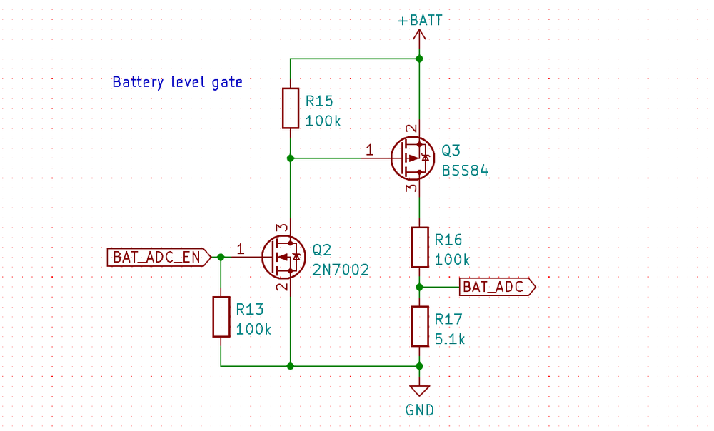
This is the part that's added to fix that. With a few extra parts the resistor divider can be completely disconnected from the battery stopping the power leakage. The software on the ESP will have to first enable the measuring circuit by toggleing a gpio, reading the value with the ADC and then disableing the gpio again. Since there's already 5.1kΩ resistors on the board I'm using another one here together with a 100kΩ. This re-use of resistor values is done since some manufacturers charge extra per distinct part model used. This brings the voltage range of the battery down to about 0-0.2v. This seemed fine at the time since the ESP has a 10-bit ADC.
With using only a fifth of the ADC range the ADC resolution is already brought down to slightly less than 8 bits. But batteries usually don't go down to zero volts. The normal voltage range is 3-4.2V giving a voltage difference of 0.06V after the voltage divider making the result slightly less than 6 bits of resolution. This does not account for ADC noise in the system yet. The result is that the final battery level graph is a bit choppy but at least it functions.

The last thing left is connectors. I added a footprint for some screw terminals for the OneWire connection. This footprint is basically the same as a pinheader except it has a fancy outline. For the battery I added a JST-PH connector because it seemed the most common one for batteries.
The I2C and SPI bus don't have standardized connectors though. But, through a bit of searching I found the pmod spec. This is an open specification made by Digilent to connect modules to their FPGA development boards. It's perfect for this usecase since the interface is just pinheaders with a defined pinout and it defines the power supply as 3.3V which I already have on the board. Some of the sensors I want are even available as pmod modules.

Getting the boards made
After laying out the PCB another complicated process begins. Getting it actually fabricated and assembled. The board has been designed that it can be hand-soldered if needed. No BGA parts are used and the _handsolder variants of the footprints are used for the common parts, which are slightly larger.
To not have vendor lock-in the board is designed to be assembled by both JLCPCB and Aisler. JLCPCB is the very cheap option in this case and Aisler is quite neat since it's actually in The Netherlands. The Aisler design rules are less forgiving than JLCPCB so I used those for the board. It mostly mean that I can't use the absolutely tiny vias that JLCPCB can drill.
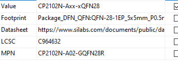
For the assembly service metadata has been added to the schematic. For JLCPCB a LCSC column was added to the part data that contains the part code for ordering from LCSC. For Aisler the parts come from the other big parts warehouses instead like Mouser. For that the MPN column is added that contains the manufacturer part number.
With this data and the selected footprints the board can be assembled. I left out all the part numberes for the through-hole parts since those are either more expensive or impossible to assemble and also pretty easy to solder manually if required on that specific board.
To actually get it made Aisler has a nice plugin for the PCB editor in Kicad: Aisler Push. With this it's just a single button and the Kicad file will be sent off to Aisler where their servers will generate the necessary fabrication files from it. From there it's using the Aisler website to fix up the MPN matching with actual parts from various suppliers and pressing order.
For JLCPCB the process is more complicated. The fabrication files have to be generated manually. There's a tutorial for going through the various steps of generating the ~10 files you need and then those can be zipped up and uploaded to the website. Since the LCSC part codes are completely unique the assembly step of this process Just Works(tm) without having to adjust anything on the website.
If Aisler had an option to specify the exact part match in the schematic metadata instead it would probably be the easiest option in this case so I hope that gets figured out in the future. Two weeks later I had the board :)

The Firmware
For the firmware of this board I just re-used the one I had previously written for one of the nodeMCU based sensor boards and extended it for the sleep features. It's pretty basic firmware that does the standard WiFi connection things for the ESP module and connects to my MQTT server to push the sensor readings in a loop.
For the battery operated boards that wouldn't be enough though. With that firmware the battery would run out in hours. There's a great series of blog posts from Oppoverbakke that go into great detail on how to optimize deep sleep on the ESP module. Especially the last post on avoiding WiFi scanning is very helpful for reducing power use.
To avoid as many delays as possible the WiFi accesspoint mac address and channel are saved into the memory of the RTC inside the module which is the only part of the chip left powered in the deepest sleep mode. Then with that information the module will save around one second of time being awake and connecting. Another optimisation is using a static ip address instead of DHCP to save another second.
I don't like having static ip addresses in my network. I have static DHCP leases for everything instead. This is why I extended the RTC connection code to do a DHCP request the first time and then save the received DHCP data in the RTC memory together with a counter to re-do DHCP after some time. This means that my board is still a fully DHCP compliant device without making a DHCP request every time it wakes up, this is what the lease time is for after all. Thanks to this I only have to power down the board when I need to change the IP address instead of reflashing it or building in some configuration web interface.
During deep sleep the whole board uses 19.1µA with a half charged battery in my tests and the transmission is down to to a bit less than a second at 70mA, but the power use of the transmissions varies quite a lot.
I had one module in production outdoors quickly to test. It sleeps for one minute in deep sleep and doesn't have any other optimisations. Looking at the data from that module it looks like it would last for about two weeks, even with the sub-zero temperatures during the night.

The battery life for the optimized version has yet to be seen. I have calculated it to be around 3 months but it would take a while to have conclusive results on that. This board uses a "3500mAh" 18650 cell which I assume in the calculations is actually 2000mAh.
Next revisions
During testing and programming I found out I had made a few mistakes with the board design. The most problematic one is that I put zener diodes on the UART lines between the USB-to-serial converter and the ESP module. This was to prevent power from the serial lines to flow into the CP2102 module and powering up that chip partially.

This did not work. When I got the boards I spend a bit of time figuring out why the programmer couldn't connect. The voltage drop through the diodes I picked is probably too much for the serial communication to work. To make things worse the diodes are completely unnecessary for this since the uart lines won't leak power in deep sleep anyway. Luckily this is easily fixable on my boards by making a solder bridge across the diodes.
Another issue on the board is that the battery charger chip gets very hot and is too close to the temperature sensor. I also forgot to add the thermal relief specified in the layout suggestions of the part so while charging that chip is practically constantly at 80°C making the value of the temperature sensor raise by around 5°C. Since this only affects the board when the battery is charging it's not a critical fault.
For cost optimization I skipped battery protection on the board. For my uses I just ordered a protected 18650 cell so it should be fine. But since I'm making a second revision board to fix these issues anyway I decided to include a battery protection chip this time around.

The protection chip sits between the ground terminal of the battery and the actual board ground and disconnects the battery pack in case of overcurrent, short circuits, overcharge or undercharge.
Another small change I did is add an extra pinheader to the board to access the UART lines directly, since pinheaders are basically free anyway.
You should make your own boards
Making boards is fun. I learned a lot during the process and now have some important skills to use in my other projects. Can you really call yourself a full stack programmer if you haven't designed the hardware yourself? :D